| 備考:Note |
https://xpslab.eng.hokudai.ac.jp/をご確認下さい |
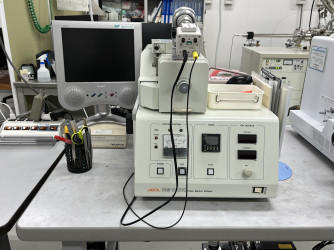
| 概要・性能:Performance |
Arイオンビームで削り出して試料の断面を作製することが出来る。機械研磨で生じてしまうようなダメージ層を形成せず、綺麗な断面を作る事が可能。細かい層構造や微粒子のSEM断面観察、EBSDの測定、AESの分析に適した断面作製できる加工装置になっている。 |
The cross section of the sample can be produced by shaving with an Ar ion beam. It is possible to create a clean cross section without forming a damaged layer that occurs with mechanical polishing. It is a processing device that can create cross-sections suitable for SEM cross-section observation of fine layer structures and fine particles, EBSD measurement, and AES analysis. |
| 仕様:Specs |
イオン加速電圧 :2~6kV
ミリングスピード :500μm/h以上 (加速電圧6kV)
試料移動範囲:X軸±3mm、Y軸±3mm
試料角度調節範囲 :±5°
最大搭載試料サイズ 11mm (幅)×10mm (長さ)×2mm (厚さ) |
Ion acceleration voltage: 2 to 6 kV
Milling speed: 500 μm/h or more (acceleration voltage 6 kV)
Specimen movement range: X-axis ±3mm, Y-axis ±3mm
Specimen angle adjustment range: ±5°
Maximum sample size 11mm (width) x 10mm (length) x 2mm (thickness) |
| 説明:Guide |
試料の断面加工をイオンミリングで行える装置です。機械研磨や切断時に生じるダメージを軽減させて、綺麗な断面を作る事が出来るので、細かい層構造や微粒子のSEM断面観察はもちろん、EBSDの測定、AESの分析に適した断面を作製することができます。 |
This is a device that can perform cross-section processing of materials by ion milling. Since it is possible to create a clean cross section by reducing the damage caused during mechanical polishing and cutting, it is possible to create a cross section suitable for SEM cross-sectional observation of fine layer structures and fine particles, EBSD measurement, and AES analysis. |