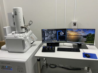
| メーカー/型番:Manufacturer/Model Name |
日本電子/JSM-IT710HR/LA
JEOL/JSM-IT710HR/LA
|
| カテゴリー:Category |
顕微鏡(電子)/走査型電子顕微鏡(SEM)
Electron Microscopes/Scanning Electron Microscope (SEM)
|
| 装置管理者:Instrument Manager |
安井 雅範
0117062404
|
| 装置所属/装置供出者:Affiliated Department/Instrument Provider |
農学部
Faculty of Agriculture
|
| 利用料金:Fee |
| 初回講習料(基本料)Initial Training Fee |
学外(他大学・公的機関) |
|
¥17,600 |
|
学外(その他・民間企業) |
|
¥17,600 |
| |
| 予約利用料Facility Usage Fee |
学外(他大学・公的機関) |
|
¥4,500 / 時間 |
|
学外(その他・民間企業) |
|
¥5,900 / 時間 |
| |
| 技術相談料Technical Consulting Fee |
学外(他大学・公的機関) |
|
¥11,000 / 時間 |
|
学外(その他・民間企業) |
|
¥14,300 / 時間 |
|
|
| 備考:Note |
J-PEAKS |
| 概要・性能:Performance |
試料表面を収束電子線で走査し、放出電子を検出して画像化する装置。ショットキー電界放出電子銃を搭載し、アウトレンズ方式を採用することで、高い被写界深度と大容量試料室を実現している。低真空モードにより、非導電性試料にも対応可能である。X線元素分析装置(EDS)を統合しており、試料の表面構造および組成の解析に用いる。 |
A device that scans the specimen surface with a focused electron beam and detects emitted electrons to generate images. It is equipped with a Schottky field emission electron gun and employs an out-lens configuration, providing high depth of field and a large specimen chamber. The low-vacuum mode enables observation of non-conductive specimens. By integrating an X-ray energy-dispersive spectrometer (EDS), the instrument is used for analyzing both surface morphology and elemental composition of a wide variety of specimens. |
| 仕様:Specs |
【走査型電子顕微鏡】
電子銃:ショットキー電界放出電子銃
対物レンズ方式:アウトレンズ方式
分解能:
・高真空モード:1.0 nm (加速電圧 20 kV) / 3.0 nm (加速電圧 1 kV)
・分析時:3.0 nm(加速電圧 15 kV、WD 10 mm、照射電流 3 nA)
・低真空モード:1.8 nm(加速電圧 15 kV、WD 5 mm、10 Pa )
加速電圧:0.5 kV ~ 30 kV(0.5 〜 3 kVは100 Vステップ可変、3 〜 30 kVは1 kVステップ可変)
照射電流:10 pA 〜 300 nA
写真倍率:×5 〜 ×600,000(128 mm × 96 mm 表示サイズ)
観察モード:高真空モード、低真空モード (10 Pa ~ 150 Pa)
検出器:二次電子検出器、反射電子検出器、低真空ハイブリッド二次電子検出器
試料ステージ:ユーゼントリック式5軸モーター駆動 (X、Y、Z,、回転、傾斜)
・可動範囲:X軸 125 mm、Y軸 100 mm、Z軸 80 mm
・回転:360°
・傾斜:-10° ~ 90°
最大試料寸法: 200 mm径 × 75 mm高さ
【エネルギー分散型X線分析装置(EDS)】
検出器素子タイプ:シリコンドラフト検出器(液体窒素不要)
検出素子面積:100 mm²
エネルギー分解能:133.0 eV以下(Mn-Kα, FWHM)
検出可能元素:Be ~ U
主な機能:定性分析、定量分析、元素マッピング |
【Scanning electron microscope】
Electron gun: Schottky field emission electron gun
Objective lens system: Out-lens type
Resolution:
・High vacuum mode: 1.0 nm (accelerating voltage 20 kV) / 3.0 nm (accelerating voltage 1 kV)
・Analytical mode: 3.0 nm (accelerating voltage 15 kV, WD 10 mm, probe current 3 nA)
・Low vacuum mode: 1.8 nm (accelerating voltage 15 kV, WD 5 mm, 10 Pa)
Accelerating voltage: 0.5 kV to 30 kV (0.5–3 kV in 100 V steps, 3–30 kV in 1 kV steps)
Probe current: 10 pA to 300 nA
Magnification (photographic): ×5 to ×600,000 (display size 128 mm × 96 mm)
Observation modes: High vacuum mode, Low vacuum mode (10 Pa to 150 Pa)
Detectors: Secondary electron detector (SE), Backscattered electron detector (BSE), Low vacuum hybrid SE detector
Specimen stage: Eucentric 5-axis motor-driven (X, Y, Z, rotation, tilt)
・Travel range: X-axis 125 mm, Y-axis 100 mm, Z-axis 80 mm
・Rotation: 360°
・Tilt: -10° to 90°
Maximum Specimen Size: 200 mm diameter × 75 mm height
【Energy Dispersive X-ray Spectroscopy (EDS)】
Detector element type: Silicon drift detector (no liquid nitrogen required)
Detector area: 100 mm²
Energy resolution: ≤133.0 eV (Mn-Kα, FWHM)
Detectable elements: Be – U
Main functions: Qualitative analysis, quantitative analysis, elemental mapping |
| 説明:Guide |
・ショットキー電界放出電子銃を搭載しており、高輝度・安定した電子ビームにより、ナノメートルオーダーの高分解能観察を実現する。
・アウトレンズ方式を採用しているため、構造的に被写界深度が深く、凹凸の著しい試料でも焦点の合った鮮明な像が得られ、立体的な試料の形態観察に優れている。
・標準装備の低真空モードにより、生物、高分子、繊維、セラミックスなどの非導電性試料の観察・分析が可能である。
・X線元素分析装置(EDS)がシステムに統合されており、形態観察と同時に視野内の元素組成をリアルタイムで分析・マッピングを行うが可能である。 |
・Equipped with a Schottky field emission electron gun, the device achieves nanometer-order high-resolution imaging through its high-brightness, stable electron beam.
・An out-lens configuration provides a structurally deep depth of field, allowing for the acquisition of sharp, focused images even for specimens with significant surface roughness, which is ideal for three-dimensional morphology observation.
・A standard low vacuum mode enables the observation and analysis of non-conductive specimens, such as biological samples, polymers, fibers, and ceramics.
・An X-ray energy-dispersive spectrometer (EDS) is integrated into the system, making it possible to perform real-time analysis and mapping of elemental composition within the field of view simultaneously with morphological observation. |
|